
TI’s radar chip’s getting us closer to autonomous vehicles

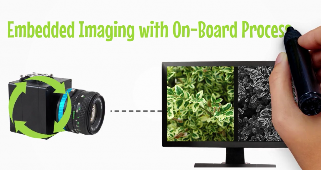
As a long-term partner with Texas Instruments  – we’ve been a Platinum Partner of the TI Design Network since 2008 – those of us at Critical Link are always interested to see what they’re up to. And as a car aficionado, the recent news about what they’ve been up to in the automotive world had special resonance for me. What they’re up to is improvements to radar.

Those who follow automotive technology news are, of course aware of the problems associated with automotive radar systems:

Traditional radar lacks resolution and can’t distinguish nearby objects. Radars are also known to sound false alarms and they consistently fail to process information fast enough to be helpful on the highway. (Source: EE Times)

On the plus side of the equation, radar tends to work well in poor weather – something that is especially important to those of us who live (and drive) under some pretty extreme weather conditions come Lake Effect Snow season. Because radar’s all-weather capabilities are so worthwhile, automotive technologists have looked to make up for the resolution problems by pairing radar with vision sensors.

TI jumped in about a year ago with:

…millimeter-wave radar chips built on standard in-house RF CMOS technology. Introduced a year ago, TI’s radar chips offer “less than 5-cm resolution accuracy, range detection to hundreds of meters, and velocity of up to 300 km/h,” according to the company.

They’ve been out with this technology for about a year, the AWR1642 mmWave are in mass production, and adoption is taking off.

Sameer Watson is TI’s GM for radar and analytic processors. He has said:

…that he expects to see TI’s radar chips inside OEMs’ vehicles “at the end of this year to mid-2019.”

(TI also has a radar chip, the IWR1642 mmWave that are designed for industrial apps.)

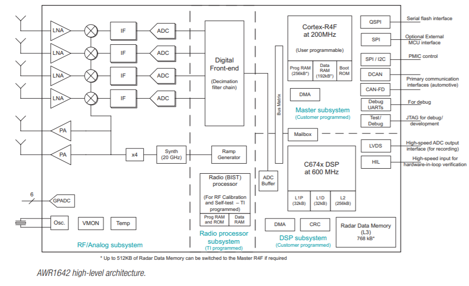
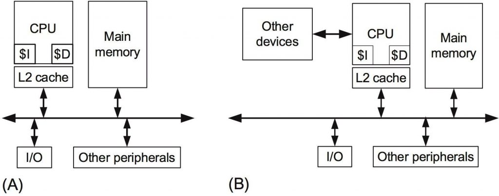
Given our roots – and appreciation for DSP technology – we’re happy to see that DSP cores, along with a microcontroller, are integrated with the radar.

The integration of the DSP turns out to be critical. It gives an almost 60% footprint reduction by improving power consumption, noted [industry analyst Cedric] Malquin. Furthermore, the DSP is central to “the signal processing chain to detect and classify an object.”

Indeed, Wasson noted that the DSP inside TI’s mmWave sensors makes it possible to classify and track objects and count people, for example. “The DSP enables users to place machine learning at the edge,” he said.

The DSP being deployed here is TI’s C674x DSP (600 MHz).

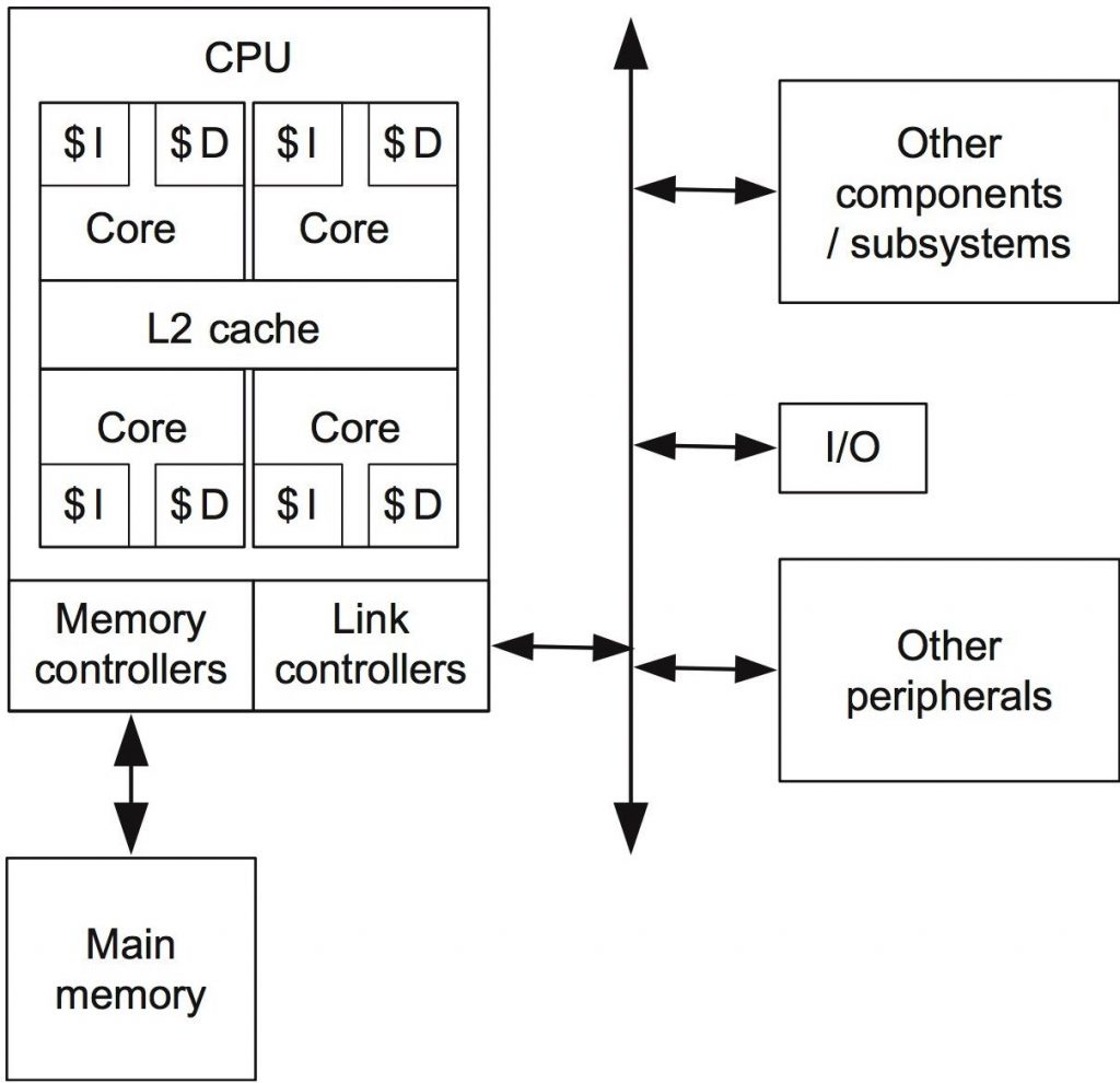
Here’s the schematic for the chip:

TI is merging radar with imaging, and imaging radar will use the radio wave data it acquires to create images.

Amazing the strides automotive technology has made over the past few years. Those autonomous vehicles are closer than they appear.

See Spot run!

I’m a dog person. I was going to say that I’m also a robot person, but that would sound like I’m saying I’m a robot. So not true! But I have been interested in robotics for a long time, dating back to graduate school. (Here’s a link to a 2015 post on the subject.) Because of these dual interests, I was of course interested in the news that Boston Dynamics’ robotic dog will become commercially available next year.

On its website, Boston Dynamics highlights that SpotMini is the “quietest robot [they] have built.” The device weighs around 66 pounds and can operate for about 90 minutes on a charge.

The company says it has plans with contract manufacturers to build the first 100 SpotMinis later this year for commercial purposes, with them starting to scale production with the goal of selling SpotMini in 2019. They’re not ready to talk about a price tag yet, but they detailed that the latest SpotMini prototype cost 10 times less to build than the iteration before it. (Source: Tech Crunch)

If you want to see SpotMini run, check out the video. It’s pretty mesmerizing to watch it, and the robot is remarkably dog-like. The video is a good indication of how sophisticated robots have become. SpotMini is pretty nimble. It can not only climb stairs, but back down them – which I’m not sure I’ve ever seen an actual dog do – at least not in my house. (There’s another video I’ve seen that shows SpotMini opening a door, which is not an idea I want to put in my dogs’ heads.)

I’m always interested in the technology that’s being used. There wasn’t a ton of info that I could find on the Boston Dynamics website, but there was this:

Spot is electrically powered and hydraulically actuated.  It senses its rough-terrain environment using LIDAR and stereo vision in conjunction with a suite of on-board sensors to maintain balance and negotiate rough terrain.  It carries a 23 kg payload and operates for 45 minutes on a battery charge.

While I find this fascinating, I won’t be trading my pups for a SpotMini. No heads to scratch. No tail wagging when you come in the door. The one advantage I can see is you don’t have to pick up after them. Other than that…


Keeping Cool with the Embr Wave

I’m always on the lookout for novel and interesting gadgets, so I was happy when a friend in Boston pointed the Wave from Embr Labs my way.

The Wave is a wearable, a device you wear on your wrist – remember your wrist? That part at the end of your arm where you used to wear a watch, but now are more likely to have something that tracks how many steps you make? Anyway, the Wave rests on the principle that if you cool or warm one place on your body, it can feel as if you’re cooling down or warming up. It doesn’t actually change your core temperature. It just makes you feel more comfortable. If you’ve 
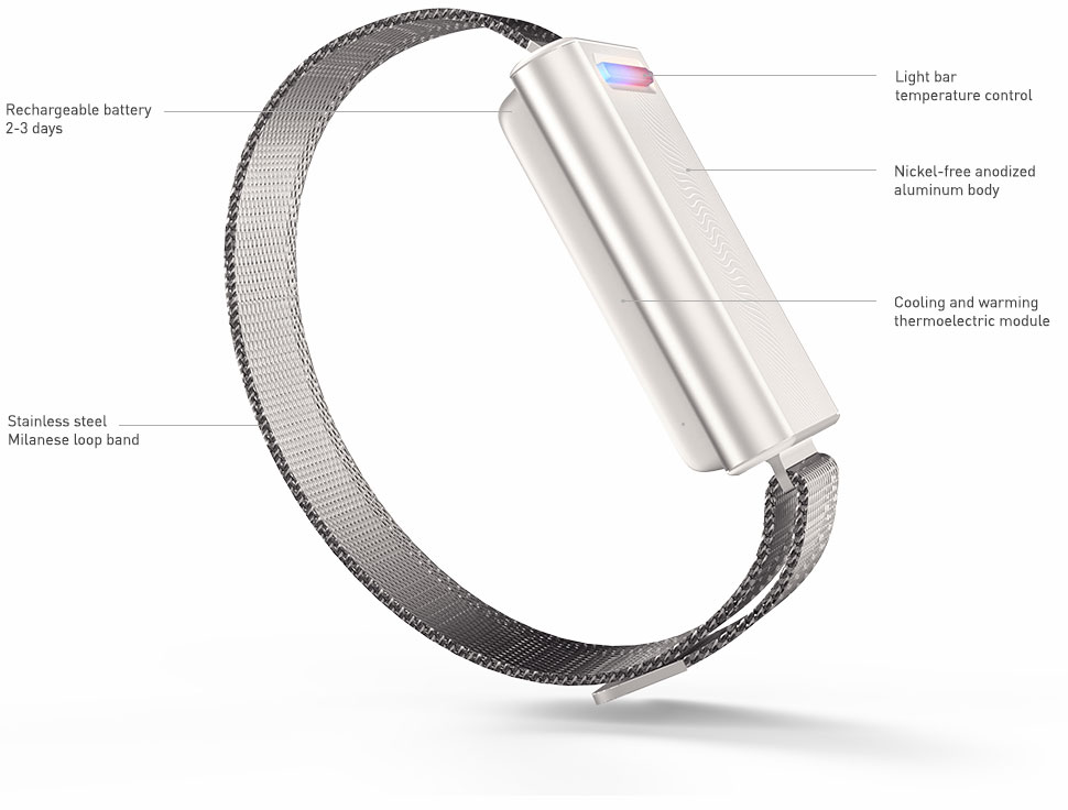
ever run cold water over your wrists on a hot day and felt instantly better, that’s how the Wave works.

It’s the brainchild of some MIT fellows, and their efforts have been funded via Kickstarter (more than $600K raised), as well as through investments from Intel and Bose, and a grant of the National Science Foundation. The product is scheduled to ship in June. Just in time to cool folks down in the summer heat. They’ve presold 4,500 Wave bracelets, which is pretty impressive, given that they go for $300 each.

The principle behind the Wave is the Peltier effect:

Named for French physicist Jean Charles Athanase Peltier who discovered it in 1834, the Peltier effect describes the phenomenon of heating or cooling caused by an electric current flowing across the junction of two different conductors. As the current moves from one conductor to another, the transfer of energy causes one side to heat up and the other to cool down. Embr Wave is basically a series of these junctions (called a Peltier cooler) powered by a small battery and attached to a wrist strap. When placed against the skin, the device makes you feel cooler by reducing the temperature of your wrist a few fractions of a degree per second for a couple seconds at a time.

That’s where the “wave” in Embr Wave comes from. Rather than providing a steady stream of heating or cooling, the device pulses with short waves of temperature fluctuation. It’s a bit counterintuitive, but according to Shames and his colleagues, this burst-based method is actually the most effective way to alter your perception of temperature and provide a sensation of thermal relief. (Source: Digital Trends)

Haiwatha Bray, the technology writer for the Boston Globe, spoke with Embr Labs co-founder Matt Smith.

Smith thinks that if enough buy a Wave bracelet, office buildings can turn down their heaters and air conditioners, saving companies millions in energy bills and easing demand for fossil fuels. (Source: Boston Globe)

This would, of course, be great, but while the Wave has many who attests to how well it works, it apparently doesn’t work on everybody. Bray is one of those it didn’t really have an impact on.  But it’s an interesting idea. $300 is a lot for a gadget, but if you’re one of those that it works on, what price comfort? I’m sort of considering it…

Embedded Computing for High Performance: Power & Energy Consumption

Over the past couple of months, we’ve been running a series summarizing the excerpts taken from Embedded Computing for High Performance by João Cardoso, José Gabriel Coutinho, and Pedro Diniz that embedded.com has published. The context for the book (and this series) is the growing importance and ubiquity of embedded computing in the age of the Internet of Things – a topic that seems to grow more important by the day. Earlier posts in this series focused on target architectures and multiprocessor and multicore architectures; core-based architectural enhancement and hardware accelerators; and performance. In this installment, we cover power and energy consumption.

The section on power and energy consumption offers information on techniques for reducing power and energy consumption. It’s pretty much the densest excerpt that we’ve seen to date, so you’re definitely advised to take a look at the entire section. But for a quick summary:

The authors set the stage by providing a number of formulae for power consumption (static power + dynamic power consumption), static power consumption, and dynamic power consumption. They then offer these tips:

The static power depends mainly on the area of the IC and can be decreased by disconnecting some parts of the circuit from the supply voltage and/or by reducing the supply voltage.

And, as dynamic power consumption “is proportional to the switching activity on the transitors in the IC”:

One way to reduce dynamic power is to make regions of the IC nonactive and/or to reduce supply voltage and/or clock frequency.

They then discuss ACPI (Advanced Configuration and Power Interface), which the operating system or applications use to manage power consumption.

Energy consumption is not directly associated with heat but affects battery usage. Thus by saving energy one is also extending the battery life or the length of the interval between battery recharges.

The authors devote next address the topic of dynamic voltage and frequency scaling.

Dynamic voltage and frequency scaling (DVFS) is a technique that aims at reducing the dynamic power consumption by dynamically adjusting  voltage and frequency of a CPU. This technique exploits the fact that CPUs have discrete frequency and voltage settings as previously described. These frequency/voltage settings depend on the CPU and it is common to have ten or less clock frequencies available as operating points. Changing the CPU to a frequency-voltage pair (also known as a CPU frequency/voltage state) is accomplished by sequentially stepping up or down through each adjacent pair. It is not common to allow a processor to make transitions between any two nonadjacent frequency/voltage pairs.

This section contains information on measuring power and energy, and on dark silicon.

We’ll be running one more installment in this series in a few weeks. After that, we’ll take a break, but will likely resume the series as embedded.com brings more excerpts of the book online.


Embedded Computing for High Performance: Performance

Recently, embedded.com ran excerpts from Embedded Computing for High Performance, a book by João Cardoso, José Gabriel Coutinho, and Pedro Diniz, which was published last spring. Performance is always a timely topic, so I’ve been devoting some posts to excerpt summaries. My first such post focused on target architectures and multiprocessor and multicore architectures; the second covered core-based architectural enhancement and hardware accelerators.

While the entire book is dedicated to performance, there’s a section – called Performance, by the way, that really drills down on the topic. And that’s the excerpt I’m addressing here.

This section begins by noting that there are myriad nonfunctional product requirements (e.g., execution time, memory capacity, energy consumption) that developers need to take into account as they devise solutions that optimize system performance. And that attention needs to be paid to identifying “the most suitable performance metrics to guide” the process by which they evaluate possible solutions.

The authors list common metrics:

  • The arithmetic inverse of the app’s execution time
  • Clock cycles required to execute a function, code section or app
  • Task latency
  • Task throughput
  • Scalability

And, in the full excerpt, further define each of these metrics.

They also provide formulae, starting with:

In terms of raw performance metrics, the execution time of an application or task, designated as Texec, is computed as the number of clock cycles the hardware (e.g., the CPU) takes to complete it, multiplied by the period of the operating clock (or divided by the clock frequency).

This is followed by formulae for the metric used when some computations are offloaded to a hardware accelerator; and speedup “which quantifies the performance improvement of an optimized version over a baseline implementation. In addressing speedup, the authors go into some detail, including an explication of Amdahl’s Law, which “states that the performance improvement of a program is limited by the sections that must be executed sequentially, and thus can be used to estimate the potential for speeding up applications using parallelization and/or hardware acceleration.”

They finish up the Performance section with a discussion of the Roofline Model “an increasingly popular method for capturing the compute-memory ratio of a computation and hence quickly identify if the computation is compute or memory bound.”

As with the other parts of this book, this excerpt is well worth the read. (And I think I’m talking myself into going out and buying the actual book.)

Just What Is Embedded Imaging

Imaging has long played a key role in industrial, scientific, medical, surveillance, and defense systems. More recently, we’re seeing imaging creep into applications that us consumers are using in our day-to-day lives – applications like hands-off parallel parking and gaming.

And while people are generally familiar with imaging, we’re often asked just what embedded imaging is.  

Embedded imaging (or embedded vision) is about incorporating camera sensors and image analysis capabilities into an electronic device. With embedded imaging, the image data and processing platform are both on board (literally) a system. Analysis and decision making can now occur in real time.  Think of the medical setting. In the “old days”, images were taken and, after the fact, interpreted by a physician. Today, with embedded imaging, an abnormality can be flagged automatically, enabling a quicker diagnosis. In the automotive world, embedded imaging is what’s making autonomous vehicles possible, interpreting images in real time and enabling the vehicle, e.g., to immediately respond to a jaywalking pedestrian.

In any case, to answer the question “what is embedded vision”, we put together a short video that offers a quick, high-level explanation. The link is here.

At Critical Link, we’ve long been involved with imaging/vision systems for these industrial-class applications. We’ve designed solutions around a broad array of image sensor technology and worked with many of the top sensor manufacturers including SONY, CMOSIS, OmniVision, e2v, Hamamatsu, Fairchild Imaging, Aptina, and Sensors Unlimited. We provide customers with embedded image processing building blocks based on FPGA and ARM, and with an array of interface options including USB3 Vision, MIPI, Camera Link, GigE Vision, among others.

In today’s world, where developers need to focus on their end application and all of the complexities that come with it, our depth of experience and hardware building blocks are proven assets in getting to market quickly and successfully.

Embedded Computing for High Performance: Enhancements & Accelerators

Embedded.com is running excerpts from Embedded Computing for High Performance, the highly informative (and, yes, educational) book by João Cardoso, José Gabriel Coutinho, and Pedro Diniz. In my last post, I summarized the initial article, which focused on target architectures and multiprocessor and multicore architectures. This post covers core-based architectural enhancement and hardware accelerators.

Core-based enhancements

In this excerpt, the authors address how CPUs have been further enhanced, beyond multicore, by incorporating more than one multicore CPU, integrated as a chip multiprocessor (CMP). They offer two ways in which CMPs can be organized.

The first is Single Instruction, Multiple Data (SIMD) units. These are:

…hardware components that perform the same operation on multiple data operands concurrently. Typically, a SIMD unit receives as input two vectors (each one with a set of operands), performs the same operation on both sets of operands (one operand from each vector), and outputs a vector with the results.

Intel microprocessors (MMX, SSE, AVX ISA extensions) have included SIMD units since the late 1990’s, and ARM got in the act more recently with SIMD extensions to ARM-Cortex (NEON technology.)

Typical tasks that SIMD units take care of are basic arithmetic and other operations, like square root. SIMD unit enhance performance by their ability to simultaneously load from and store to memory multiple data items, taking advantage of the entire width of the memory’s data bus.

One bit of advice the authors offer:

To exploit SIMD units, it is very important to be able to combine multiple load or store accesses in a single SIMD instruction.

The second option for organizing CMPs presented is Fused Multiply-Add (FMA) units.

Fused Multiply-Add (FMA) units perform fused operations such as multiply-add and multiply-subtract. The main idea is to provide a CPU instruction that can perform operations with three input operands and an output result.

Both Intel and ARM have microprocessors that include FMA.

Hardware Accelerators

Here the authors discuss two types of hardware accelerators, GPU accelerators and reconfigurable hardware accelerators (absolutely something we’re quite familiar with here at Critical Link).

GPU accelerators were initially used for graphical computation, but these days they also support additional application areas, including scientific and engineering apps. Then there’s our friend, the reconfigurable hardware accelerator:

Given the ever-present trade-off between customization (and hence performance and energy efficiency) and generality (and thus programmability), reconfigurable hardware has been gaining considerable attention as a viable platform for hardware acceleration. Reconfigurable devices can be tailored (even dynamically—at runtime) to fit the needs of specific computations, morphing into a hardware organization that can be as efficient as a custom architecture. Due to their growing internal capacity (in terms of available hardware resources), reconfigurable devices (most notably FPGAs) have been extensively used as hardware accelerators in embedded systems.

The authors give a shout out to components that combine FPGA and DSP. As I said, right up our alley. Here’s a block diagram of a reconfigurable fabric that includes both FPGA and DSP. It doesn’t look anything like the sort of block diagram we’d present to a client, but I had my reasons for including it here.

As with my earlier post, I encourage readers to head over to embedded.com to read the full excerpts (which are all accompanied by ample diagrams and other illustrations).

Embedded Computing for High Performance: Architectures

Spurred on by the explosion of interest in the Internet of Things, there’s been an explosion of interest in embedded systems. Because of this, Embedded.com is running excerpts from Embedded Computing for High Performance, a recent book by João Cardoso, José Gabriel Coutinho, and Pedro Diniz. In this and my next few posts, I’ll be briefly summarizing these excerpts (and encouraging all readers to read the articles in their entirety, as there’s a lot to learn in them and the writing is clear and straightforward). The first two articles focus on architecture: target architectures and multiprocessor and multicore architectures.

Target architectures

The authors acknowledge right up front something that those of us at Critical Link have been experiencing first hand throughout our history:

Embedded systems are very diverse and can be organized in a myriad of ways. They can combine microprocessors and/or microcontrollers with other computing devices, such as application-specific processors (ASIPs), digital-signal processors (DSPs), and reconfigurable devices (e.g., FPGAs [1,2] and coarse-grained reconfigurable arrays—CGRAs—like TRIPS [3]), often in the form of a System-on-a-Chip (SoC).

Here’s their diagram of a standard single CPU architecture. (Looks pretty familiar!)

In their article, the authors take a look at a decades-long history of how performance improvements have come about, and discuss the tricks of the trade (code optimization, parallelizing sections of code) that engineers deploy to meet requirements.

They then address extending simple embedded systems like the one depicted above “by connecting the host CPU to coprocessors acting as hardware accelerators,” such as an FPGA and network coprocessors.

Depending on the complexity of the hardware accelerator and how it is connected to the CPU (e.g., tightly or loosely coupled), the hardware accelerator may include local memories (on-chip and/or external, but directly connected to the hardware accelerator). The presence of local memories, tightly coupled with the accelerator, allows local data and intermediate results to be stored, which is an important architectural feature for supporting data-intensive applications.

They then offer the reminder that hardware accelerators come with overhead: the cost of data movement between the accelerator and the host processor, so they offer different approaches with less communications overhead.

Multiprocessor and multicore architectures

Modern microprocessors contain a number of processing cores, each (typically) with “its own instruction and data memories (L1 caches) and all cores share a second level (L2) on-chip cache.” Here’s the authors’ diagram of a standard multicore (quad-core CPU) architecture. (Looks pretty familiar!)


In the article on multiprocessor/multicore, the authors also talk about platforms that extend commodity CPUs with FPGA-based hardware.

I’ve just skimmed the surface here, but wanted to give a flavor on the types of information provided in these articles. Admittedly, it’s all textbook stuff, but if you’re interested in high performance embedded systems (and if you’re reading this post, you probably are) you may want to go over to embedded.com and read the articles through in their entirety.

In my next post, I’ll be summarizing the excerpts on core-based enhancements and hardware accelerators, but feel free to jump ahead and take a look at the full excerpts.

Medical Device Security in the News

Today is Valentine’s Day, so I guess it’s appropriate to write a heart-related post.

What prompted it was a piece I saw on EE Times a week or so ago. In a post entitled “Implants Raise Security Awareness,” Joanne Emmett addressed the topic of medical device security. She started by going back a decade to the time when the doctors who were giving then-Vice President Dick Cheney a heart defibrillator replacement “ordered the device’s manufacturer to disable its wireless capacity.” There were concerned that the device could be hacked, and Cheney assassinated via technology. In a weird case of art imitating life, in an episode of the thriller Homeland, the serial number of the fictional VP’s pacemaker is stolen and a terrorist uses the information to rev up the pacemaker, triggering a fatal heart attack.

More than a decade on, the security of networked medical devices is a serious concern for many reasons. Concerns are growing as devices are engineered to gather and report increasing amounts of data, most of it collected and transmitted using widely available, off-the-shelf software. (Source: EE Times)

As Emmett points out, the real worries aren’t about attacks on individuals like Vice President Cheney or the VP on Homeland. They’re around data mining, and using the information for financial gain.

Hacked data can reveal commercially valuable information, such as performance data on competitors’ products. Such data can be used to exploit weaknesses in a rival’s marketing or used to modify the company’s own offerings.

Networked devices provide feedback on a wide range of patient data such as blood pressure, respiration, blood enzyme levels, and other health conditions. Insurers that issue individual life insurance policies often purchase this information — repackaged by third parties to be of apparently legitimate origin — to assess clients for insurability and to set premiums.

She also notes that fitness devices, like Fitbits, also produce large quantities of biometric information.

The FDA has released some guidance on cybersecurity for medical devices, and legislation has been introduced that would “codify protections for medical device data.”

Emmett’s post was particularly timely given the recent news that fitness device data, from devices worn by U.S. soldiers, could potentially be used to identify their locations. Heat maps developed by Strava, a GPS tracking company, aren’t real-time depictions, but could help enemies figure out sensitive information. When the heat maps show affluent regions in the United States and Europe, where so many millions of people wear fitness trackers, the picture is pretty dense. In poor regions in the Mideast and Africa, where fitness consumers are few and far between, what shows up on the maps are the areas where Fitbit-wearing soldiers congregate.

An Australian student was the first to notice that a heat map of Syria showed where soldiers congregated. A journalist found information that likely gives away the location of a CIA base in Somalia. A Twitter use claims that “he had located a Patriot missile system site in Yemen.” (The heat map shown here is of Kandahar Air Force Base.)

The U.S.-led coalition against the Islamic State said on Monday it is revising its guidelines on the use of all wireless and technological devices on military facilities as a result of the revelations.

“The rapid development of new and innovative information technologies enhances the quality of our lives but also poses potential challenges to operational security and force protection,” said the statement, which was issued in response to questions from The Washington Post.

“The Coalition is in the process of implementing refined guidance on privacy settings for wireless technologies and applications, and such technologies are forbidden at certain Coalition sites and during certain activities,” it added. (Source: Washington Post)

Technology that both “enhances the quality of our lives” while at the same time posing “potential challenges” pretty much sums up the Internet of Things when it comes to the consumer end of the product spectrum. There may not be someone out there who’s going to hack someone’s pacemaker and throw them into cardiac arrest, but a lot of the security challenges that have been addressed in the industrial IoT have yet to be seriously taken when it comes to consumer devices, including some life and death ones.


Rick Merritt’s Top Innovations for 2017 (from EE Times)

(Seriously, how could I resist an article with the subhead “Engineers march toward progress”?)

That reference to marching was actually a nod toward April’s March for Science, which Rick named the 8th best innovation of the year, which he saw as “a pent-up desire to celebrate technology, the scientific method and the people who honor and practice it.” After that, he jumped right into a round-up of some interesting technology that, in many case, is relevant to the work that we do at Critical Link.

In 7th place he named Microwave-Assisted Magnetic Recording, the hard disk drive industry’s “reinvent[ion of] its core technology. We sometimes forget about some of the fundamental infrastructure – like all those HDDs out there – make a lot of more interesting and cool stuff possible.

Samsung’s 3D NAND and Intel’s 3DXP made it to Rick’s 6th place, and he gives Samsung most of the credit here.

Over the last few years Samsung’s engineers showed the world a new kind of 3D design and manufacturing. It has not only revolutionized NAND flash but become the poster child for a kind of monolithic 3D design likely to become a mainstay for the semiconductor industry for many years to come.

5th place goes to RICSC-V Instruction Set Architecture, work done at Berkeley “in the past few years to spawn a new microprocessor architecture unencumbered by royalties. Their efforts also sparked new possibilities for open source hardware.” When we think open source, we’re mostly thinking software, but a royalty-free microprocessor architecture has some interesting possibilities.

Rather than heap more praise on Amazon’s AI speaker – ‘Alexa, you’re so wonderful’ – Rick points out the Baidu DUEROS voice assistant which was arguably out there before Amazon. Baidu’s voice assistants “just happened to speak Mandarin so a lot of people in the U.S. didn’t notice them.”’ Point taken.

Nvidia’s Volta GPU is Rick’s third-best innovation for 2017. This is a chip tailored for training neural nets.

Volta beat enterprising startups such as Nervana and Graphcore to market and is getting raves from AI researchers putting the chip through its paces. This is the best of a big company watching the horizon and nimbly responding.

Mark me down as someone intrigued by the potential of neural networks. And speaking of neural networks, second place is held by Google’s Tensor Processing Unit. Initially “designed to speed inferencing jobs for deep learning neural networks,” it’s not been updated “to handle training jobs.” Google also gets kudos from Rick for disclosing much of the IP behind their first-gen TPU chip.

Rick’s first place for innovation goes to Extreme Ultraviolet Lithography, which I’ve seen referred to as the technology that’s going to extend the life of Moore’s Law, is what semi manufacturers will use once optical lithography runs its course.

After more than 20 years in development, ASML shipped this year what it called volume-production-ready versions of some of the largest and most expensive electronics gadgets ever built. If the new EUV steppers succeed, they will help others build bleeding edge electronics devices for several years to come.

Rick notes that this EUV need some refinement, but it sure sounds like a game changer.

I like Rick’s list a lot. When I get some free time, I’ll think about what I would add to/delete from him. Or maybe I’ll just start keeping a closer eye out for the innovations that are happening in 2018, now that we’re one month into the year…