Score! Goal Line Technology Comes to the World Cup

The World Cup, which this time around is coming to Brazil, will be underway by mid-June.

Most of the buzz around it has been the question of whether Brazil will be ready.

What’s been getting less buzz is the technology that will be in place. For the first time, goal-line technology will be used to clarify those situations where goals are too close to call – but have, historically, been called anyway.

Everybody isn’t happy about the use of goal-line technology. Many are concerned that this will lead to what is a fluid game turning into a stop-start game where every play is subject to review.  I’m not going to argue that the NFL doesn’t put a stop-start game on the field, but they do manage the review process by limiting challenges, and making unsuccessful challenges bear a penalty. (There’s also some fear that using the technology will take all the fun out of post-game rehashes and arguments.)

Anyway, I’m more interested in the technology than the politics.

The system that will be used is from GoalControl-4D, a German company which beat out Hawk-Eye Innovations, which had technology that was used last season in the English Premiere League. Like Hawk-Eye:

GoalControl-4D also deploys 14 high speed cameras strategically located around the stadium roof or galleys and directed at the goals. They are connected to a powerful image processing computer system that tracks the movement of all objects on the pitch and filters out the players, referee, and any other objects save the ball. The system knows its three-dimensional x-, y-, and z- position to within a few millimeters in the coordinate system of the pitch. Again, when the ball passes the goal, the system instantly sends an encrypted signal to the officials’ specially modified wristwatches. (Source: EE Times)

Security, not surprisingly, is a big deal. Easy to imagine the nightmare scenarios if the system got hacked.

The GoalControl-4D is expected to cost $260,000 per stadium to install, and $3,000 per match to operate. Interestingly, and perhaps controversially, he added, “an important fact to point out is that our transmission code of the sender is extremely secure and has a frequently changing encrypted code. Contrary to our British competitor, we are not using the Wi-Fi/LAN frequency band of 2.4GHz. This frequency bears many disadvantages and security risks regarding the system. Just think how many access points and smartphones are in the stadiums during the matches which are all sending on the 2.4GHz frequency.”

Anyway, it will be interesting to see if there are any controversies settled – or started – by the deployment of the goal-line technology.

What’s up with NAND?

3D NAND is on the way, but it’s not going to be here tomorrow.

Last week, Toshiba and SanDisk announced that they were jointly investing in a production facility in Japan, coming on line in 2016. This will be good news for smartphone and other mobile device users: the storage capacity of 3D NAND will be 16 times greater than what’s in there now.

While the transition to 3D NAND gets underway, SanDisk and Toshiba will be revving up the interim technology.

SanDisk’s 1Z-nm technology will be applied to both 2-bit-per-cell and 3-bit-per-cell NAND flash memory architectures with production ramp to begin in the second half of 2014. The 15nm technology scales chips along both axes, and will be used across a broad range of SanDisk offerings, from removable cards to enterprise SSDs.

Toshiba’s new process replaces its 19nm process technology, and is aimed at providing a transitional step to 3D NAND, said Scott Nelson, senior VP of Toshiba America Electronic Components’ memory business unit. Toshiba’s 15nm process works in conjunction with improved peripheral circuitry technology to create chips that achieve the same write speed as chips formed with second generation 19nm process technology, but boost the data transfer rate to 533 megabits a second — 1.3 times faster — by employing a high-speed interface. (Source: EETimes)

​Just as NAND is used in SSD’s (in place of a platter based hard drive), in the embedded world they are used on-board to hold a file system. The increased speed is great, as it improves the performance of apps that require reading large volumes of data from the file system. But NAND is inherently prone to bit-errors. The controllers correct for it, but over time and wear, the bit-errors grow.  As the geometries get smaller, the density of bit-errors gets higher, but – as the article goes on to point out – the controllers are getting better faster than the error rate is growing.

Embedded applications really benefit from enhanced longevity. Certainly, the apps Critical Link works with aren’t throwaways that get tossed when the next new thing comes along. Allowing for more write cycles before wearing a sector out, wear leveling drivers have helped a lot with longevity improvements. The consumer market can deal with more errors and shorter longevity. As often as not, cell phones are traded in when the next upgrade becomes available. Let’s face it, the cell phone providers have us addicted to our next upgrade, and the next re-up of our cellular contract that results.

So here’s a prediction for you: when the 3D NAND starts hitting the market, the lure of storage capacity that’s increased by more than an order of magnitude will have consumers clamoring for upgrades. Think of all those movies you’ll be able to store on your smartphone!

Forget a better mousetrap, what the world needs is a better battery

In a recent Atlantic Monthly, there was a brief, but interesting, article on batteries, in which journalist James Fallows asked Nobel-winning physicist Steven Chu and Yi Cui, who is a battery researcher, about the importance of building a better battery.

You don’t need me to tell you about the importance of batteries. They’re essential to all those electronic devices – laptops, smartphones, tablets – that have become so critical for 21st century life. They’re also an important (and, at present, to some extent a limiting) factor with respect to more widespread adoption of electric cars. And then there are the “utility-scale batteries” needed for renewable energy sources:

Utility companies will need batteries to stabilize the flow of renewable energy into the grid, plus a better electrical control system to do the switching. People may have these batteries at their houses instead of generators…

…There is a slow march toward improving today’s systems, by 5 or 10 percent a year. Meanwhile, many innovative companies, scientists, and engineers are exploring novel approaches. Many of them may not work. But there is a reasonable chance that a couple may work—and really work, to double or triple energy density and lower cost. If you are a battery company and your cost per unit of storage doesn’t drop by a factor of two in the next five years, you are going to be out of business. (Source:  Atlantic Monthly)

One of those “novel approaches” was announced last year by researchers at the University of Illinois, who:

… have developed a new lithium-ion battery technology that is 2,000 times more powerful than comparable batteries. According to the researchers, this is not simply an evolutionary step in battery tech, “It’s a new enabling technology… it breaks the normal paradigms of energy sources. It’s allowing us to do different, new things.” (Source: Sebastian Anthony of Extreme Tech.)

As electronics engineers, those of us at Critical Link like to stay on top of what’s happening in the battery world, out of both general interest, and because of the implications that battery development holds for the applications that our clients develop.

Critical Link has a long history with defense applications, and battery life is a huge issue for future defense programs. One example: we’ve done work on mesh networking for defense applications, which can enable networks of unattended sensors in the field. Unattended networks have a lot of advantages to the warfighter…persistent eyes, ears, and even noses in the field without putting soldiers at constant risk. But what good is that if you have to physically get to each sensor to change the battery every few days?

We’ll be following the “better battery” story closely. From our viewpoint, it’s a lot more important than someone building a better mousetrap (at least to those of us who a) don’t have mice; b) still know how to bait the old spring trap).

Robotic milking. (Yes, technology is everywhere.)

Even though I live in upstate New York, where there are plenty of dairy farms, I don’t spend a whole lot of time thinking about where the milk on my cereal and the cream in my coffee comes from, other than that it comes from cows. But I do spend a lot of time thinking about technology, and how it’s being used in so many different ways. So I was intrigued by a recent article in The New York Times on robotic milkers.

Now milking machines have been around for over one hundred years, and even the more automated and robotic milkers have been used for a while, but, as technology gets more and more sophisticated, so do those robots.

“Robots allow the cows to set their own hours, lining up for automated milking five or six times a day — turning the predawn and late-afternoon sessions around which dairy farmers long built their lives into a thing of the past.

“With transponders around their necks, the cows get individualized service. Lasers scan and map their underbellies, and a computer charts each animal’s “milking speed,” a critical factor in a 24-hour-a-day operation.

“The robots also monitor the amount and quality of milk produced, the frequency of visits to the machine, how much each cow has eaten, and even the number of steps each cow has taken per day, which can indicate when she is in heat.” (Source: NY Times.)

robotic milking

Okay, so maybe that last bit was too much information, but this is a very interesting application of vision systems and other technology.

Anyway, I was interested enough to spend a bit of time grazing (sorry!) around the sites of a couple of the companies that make the robotic milking equipment.

One of the ones I looked at, Lely, has a robotic milker called the Astronaut – can’t imagine where that name came from – and part of their value proposition is that “the cow is key”, and that the Astronaut is “the natural way of milking.” Well, I don’t know exactly how “natural” a robotics milker is ever going to be, but it probably is the future way of milking. By the way, I figured out that they do ARM based processing – what processors they use I couldn’t tell you.

What I can tell you is that those robotic milking machines have come a long way from the 4H kid sitting on stool, milking by hand.


Embedded Design Trends

Last week, EE Times had an interesting piece by Rick Merritt that catalogued ten trends in embedded design. The trend results are from a survey that was taken earlier in the year.  (Here’s the link where you can see the full list and the underlying survey data it’s based on.)

The first trend found is that, while WiFi is still “twice as popular as the second most used wireless transport”, which is Bluetooth (LE/Smart), as is number three (Bluetooth classic), Bluetooth is gaining ground and momentum. We’ve seen this demand, and we have a Bluetooth expansion kit (based on LSR’s TiWi-R2 Transceiver Module) for our MitySOM-335x development kits.

Another trend: more multi-processing, with an even, 50-50 split between the single processor camp and those with designs based on multiple processors. The average number of microprocessors employed among respondents was 2.4. (Four percent of respondents used more than ten!) Our customers are part of this trend, with a number using the MityDSP-L138, which features a dual core (ARM-DSP) processor.

And it looks like 8-bit processors are on the way out. (Sixteen-bit, too.) Nearly two-thirds of current designs use 32-bit processors. This is certainly consistent with what we see among our customers. What we haven’t seen so much is the trend that EE Times spotted: the steady decline in the use of FPGA, which has decreased in use “from 45% six years ago to 31% last year, rising very slightly this year to 32%.” We’re advised to “Stay tuned to see whether we have we hit the bottom or the decline continues.” We’ll be on the lookout among our customer base, too, but we’re still seeing a fair amount of interest in FPGA’s.

A trend which caught our eye was the one that noted that “skeds are slipping.”

…respondents said their embedded design teams are getting a little smaller and slipping schedules more often. In 2014, 41% of all projects finished on schedule or ahead of schedule, and 59% finished late or were canceled.

Not to blow our own horn too loudly, but one of the best ways to deal with smaller teams and slipped schedules is to use a SoM from Critical Link!

Behind the high-speed trading scenes

With the publication of Michael Lewis’ new book, Flash Boys, there’s been a lot in the news lately about high frequency (or high speed) trading. (For those who aren’t familiar with Lewis, he is also the author of a couple of very good sports-related books – Moneyball and The Blind Side – that were made into a couple of very good sports-related movies – as well as of Liar’s Poker, an earlier book about Wall Street.)

I’m not going to get into Lewis’ argument – that high frequency trading, which exploits a 1-2 millisecond – and even fraction of a millisecond – advantage in transmission speeds from exchange to exchange, basically rigs the game.

What’s really interesting about this, from my point of view, is what’s going on behind the scenes with the systems that enable the trading, which often rely on FPGAs.

PC Magazine had an article by Mitchell Hall on this last fall that did a good job explaining things:

 On a basic level high-frequency traders use a combination of hardware and software to see how much someone else is willing to buy or sell a given security for fractions of a second before their competition does. They can then trade accordingly. It’s almost like being able to bet on a horse race from the future; you already know who’s crossed the finish line first.

While software algorithms play into things, the real advantages come on the hardware side and the drive for zero latency:

High-frequency trading is at the forefront of hardware acceleration. This means using hardware-accelerated network stacks and NPUs (network processing units), or custom-designed FPGAs. NASDAQ offers its ITCH data feed processed by an FPGA instead of a software stack. “Some people have put market data processing into an FPGA,” says [former high-frequency trader David] Lauer, “some people have put trade logic into an FPGA, risk controls into an FPGA; some people are using GPUs to do massively parallel analysis on the fly. So there’s some pretty interesting stuff going on in hardware acceleration that I think is more cutting edge than most industries.”

FPGAs have been around for about 30 years. Interesting that they still remain such a workhorse, isn’t it?

RIP XP, and what this means for embedded solutions

While you’re probably not likely to be running Windows XP on your own PCs (maybe other than the one in the kitchen you use to pay the bills on), there are an awful lot of XP’d up computers out there. I saw a recent article in The Wall Street Journal Online that put the number at 300 million,

… including many that manage water, electric and sewage treatment plants and ATMs.

This is important because Microsoft has end-of-lifed XP. No more updates, no more security patches. Which is bad news for those 300 million computers, which will now be ultra-vulnerable to new security threats.

The software giant itself will further contribute to the problem in May, when Microsoft issues updates to Windows 7 and Windows 8, more modern operating systems built on a similar blueprint as XP. The patches Microsoft sends for those operating systems will be pointing hackers to possible weak spots in XP without supplying the fix.

Just as there will be enterprising hackers out there, I’m sure that some enterprising good guys will jump in to help solve potential security problems and/or to help migrate those who have critical applications (like water, electric, sewage treatment, and ATMs) that have embedded PCs to embedded systems with more of a shelf life. Even if this happens – which it no doubt will – the end of XP still represents a big concern.

XP, for a number of reasons (including the security holes and frequent patches) was a pretty poor embedded solution to being with. In general, PC-based boards have low longevity. This means that customers get whip-sawed by frequent changes, and the need to requalify a product when the PC-based boards get swapped out, which can cause Windows driver compatibility issues, among other potential problems.

Anyway, from our point of view, XP going away may well force more folks off of embedded PCs, and onto ARM or DSP-based SoMs.

This works for me…


Moore’s Law (To Infinity and Beyond?)

Moore’s Law  – “the number of transistors incorporated in a chip will approximately double every 24 months” –  has been around now for 50 years. (Look for Intel, and the semiconductor industry, to make a big deal of this, come 2015.) It has stood up pretty well over time, in part because the industry has used it as a goal, and keeping Moore’s Law going pretty much drives R&D across many segments of the computing industry.

There’s been some questions around whether Moore’s Law will continue to be operative as a rule of thumb because of thermal power, and transistor interconnect, constraints.

Then along comes some MIT research – maybe even in anticipation of the Golden Anniversary of Moore’s Law – that suggests that Moore’s Law may not be running out of steam.  They believe “that they have found a way to enable semiconductor manufacturers to continue shrinking geometries below 20 nanometer and produce advanced components cost effectively.” (Source: article by Ismini Scouras in EE Times,)

The researchers:

…have developed directed self-assembly (DSA) techniques that they claim resolve the issues associated with the two main lithography techniques used in the semiconductor manufacturing process today — photolithography and electron-beam lithography. Photolithography at 193-nm is reaching its limit with feature sizes around 25-nm. And the throughput in electron-beam lithography, which can produce smaller features, is insufficient for sub-20-nm resolution pattering over large areas.

According to Caroline Ross, who is a professor of Materials Science and Engineering at MIT,

 “Nanoimprint lithography may also be a viable process. Each of these has its own limitations and advantages, but overall DSA is a very attractive option because it provides scalability at high throughput and a lower cost than other processes.”

When I consider of how the processing footprint has decreased during my career, it’s been extraordinary to begin with. To think about it continuing on into the foreseeable future is pretty exciting.

Reminds me of Buzz Lightyear: to infinity and beyond!

Billions and billions of things

In late February, the Mobile World Congress was held in Barcelona.

No, I wasn’t there, but since I’m both personally and professionally interested in the Internet of Things, I did enjoy reading about what went on there.

One article I saw – The Internet of Things: 50 Billion is Only the Beginning (by Pablo Valero, in EE Times) – cited a Cisco prediction – considered by many conference pundits to be conservative – which forecasts that:

…we will have over 50 billion connected devices by 2020. This number is considered bullish by some, but cautious by most. With almost 7 billion cellphones active in the world already, within six years we could have an almost unlimited number of connected devices.

Since the world population in 2020 is pegged at about 7.5 billion, this will translate into between six and seven devices per person. I know, I know, it doesn’t work that way.

But all I can say is that I will be responsible for more than my proportionate share of things IoT.

Anyway, this prediction of 50 billion connected devices is staggering. It’s hard to imagine. Just wow.

It’s amazing to think about what will be smart in the future, and the new sorts of things that people will be dreaming up.

One of the concerns surfaced in the article is that:

The lack of standards is one of the main barriers to mass adoption of connected devices, they agreed…Many players are developing their own M2M and IoT networks, effectively creating a Tower of Babel that will make it difficult to manage and connect all these devices.

One example of where interoperability standards are emerging is 6LoWPAN (shorthand for IPv6 over Low power Wireless Personal Area Networks). 6LoWPAN standards are aimed at ensuring that even small, low power devices will be able to be part of the IoT.

Fifty-billion devices participating in IoT.

Wow!

Google’s Modular Smartphone

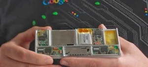
For those of us who like gadgets, like to tinker, and like the idea of smartphones getting even smarter, there’s good news: Google is continuing to work on the Ara, a modular smartphone.

Project Ara is essentially a set of electronic components that can be placed together to create a completely customizable mobile phone. If you want a cellphone with a keyboard and smaller screen, you will simply be able to select those components and clip them onto a base called an endoskeleton. Maybe you want a better camera but smaller battery: Just pbits-ara2-tmagArticlelug those in instead. (Source:  NY Times Bits blog)

If the Project Ara experiment pans out, Google plans on offering three different sizes: a mini version, a medium (pretty much the size of a current smartphone); and a jumbo. They’re also hoping that this takes off with third-party developers who will jump in to create plug and play components.

The ability to choose the features you want, and to be able to build up as you go along, is a very cool idea. While – despite the intention to offer this in a mini format – I don’t think that this method is likely to result in the smallest phones of all time, but it will allow for the ultimate phone customization.

This is probably a long way from being a mature, ready-for-market product, but it will be interesting to see how they answer some of the questions I have: how will the OS know what modules are installed? How long before the OS is robust enough to deal with devices that are and are not there, depending on the phone configuration?

Anyway, I can definitely see myself tinkering with one of these!