
Some cool new cooling technology

It’s summer, so we expect it to be hot. Just not as hot as it’s been around the country of late. Even up here in the north country, where we’re more used to extreme weather winters than extreme weather summers, it’s been too darn hot.

And so, we do whatever we can to stay cool.

If we’re fortunate enough to afford it, we sleep with the window air conditioner humming away in the bedroom. When we wake up in the morning, we hop in our car and rev up the air conditioning for the drive to our AC’d office.

If you live and work in Syracuse, that drive to work may well take you through Carrier Circle, passing by the massive Carrier facilities where for many years, air conditioners were manufactured. Although they’re no longer building AC’s in Syracuse, Carrier remains the world’s largest producer of air conditioning units. And it was Carrier that largely made possible the expansion of the use of air conditioning, which continues to grow worldwide. As the planet heats up, demand for AC will continue to increase.

It’s been estimated that, by 2050, there will be 4.5 billion air conditioning units in place around the world, and they’ll be responsible for consuming 13 percent or so of all electricity. There’s a feedback loop in play here: the more air conditioning used, the more its use will contribute to climate change – with the higher temperatures and longer heat weave that will bring – which in turn will result in accelerated demand for air conditioning. All this to ponder while taking into consideration that the fundamental technology used in air conditioning hasn’t changed all that much since the 1940’s, when AC’s popularity began really taking off.

But there are a number of new approaches to air conditioning in the works, and I recently came across a roundup of some of the emerging ideas in an article by Robin Fearon that appeared on Discovery.com.

Some of the suggestions aren’t particularly reliant on sophisticated technology. Plugging air leaks in buildings, greater use of insulation, and covering the roof areas of buildings with white reflective materials will result in a lot less energy use, saving both money and the environment.

The vast majority of American households have AC units. Today’s air conditioners are more energy-efficient than they were in the past but, Fearon asks, “what if each unit captured carbon dioxide from the air and converted it into renewable hydrocarbon fuels?” The hydrogen extracted from carbon dioxide and water from the air could be turned into liquid synthetic oil: carbon-free energy!

Energy-efficiency could be improved with “hybrid technologies that transfer heat between semiconductors or use magnetic fields.” Performance would be increased by a factor of 4 or 5.

There are a number of ideas being explored for reducing, or getting rid of entirely, hydrofluorocarbon refrigerant use in AC’s.

Alternatives include using low-cost solid-state non-toxic ‘plastic crystals’ and a moisture storage battery assembly that dries the air first, making it easier to cool.

Another idea being considered uses a bult-in solar panel to power a unit’s compressor and heat exchanger.

Alternative cooling technologies such as ground source and dual-source heat pumps that draw on ground and air temperature exchange to cool buildings are also increasing in popularity. In winter they warm buildings using ground heat and in summer they pump heat out of buildings into the ground and surrounding air.

Grid technologies are also getting cleaner and smarter, with more use of renewable sources of energy coming to the fore. Within buildings, improved control systems and sensors are being deployed to minimize energy need. (E.g., if there’s no one working in an area, there’s no need to keep that area cool.)

What else is in the works?

Penn State has a thermoacoustic chiller “which uses soundwaves and helium to lower temperatures.” Then there are:

…mirrors that simply bounce heat radiation out into the cold reaches of space, reducing the energy needed to cool structures by up to 70 percent.

There’s a lot happening that will make it possible for us to keep cool without making environmental conditions any worse.

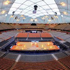
Meanwhile, for Syracuse folks and/or fans of Syracuse University basketball, the Carrier Dome, which for more than 40 years was the site of SU basketball (and football and lacrosse) games, has acquired a new name. It’s now the JMA Wireless Dome. The Dome has recently been refurbished and now, for the first time, it’s got air conditioning. (From Carrier, I assume…)

Silicon Photonics: helping Moore’s Law keep up

EE Times has been running a special project (More on Moore) dedicated to exploring options for increasing chip “power, performance, area, cost and speed to market” now that the scaling that Moore’s Law predicted (i.e., the number of transistors on an IC doubles every couple of years) is stalling out a bit. My most recent post focused on their articles on packaging approaches that support heterogeneous design and integration as one of the “new design and production paradigms” that are emerging. With this post, I’ll take a look at their second option: silicon photonics.

Silicon photonics is attractive because it can increase data transfer between and within chips without consuming as much power and generating as much heat as traditional all-electronic circuits. With the increasing demands placed on bandwidth, there’s a need for this sort of energy-efficient scaling. Silicon photonics doesn’t replace electronics but, since silicon is already used in IC’s, it can be used to create hybrid components that combine both optical and electronic approaches in a single chip. No new semi fabrication techniques are required. And Moore’s Law gets to keep on keeping on.

Silicon photonics has been around for a while – twenty years now – and is wending its way from being used in data centers and “industrial strength” applications into the consumer realm.

Yole is a research organization that has been keeping an eye on silicon photonics for the past decade. In their December 2021 EE Times article, Yole’s Eric Mounier and Alexis Debray provided a synopsis of where they see the market going for this technology. A decade ago, datacom was its primary market, and the overall market was small (estimated at only $65M). In 2020, they pegged the market at $87M.

Today’s landscape has shifted.

Today, dynamized by cloud applications for home office and personal use, video on demand, and 5G expansion, the primary silicon photonics application is still optical communication, with the technology integrated into 25% to 30% of optical transceivers. Some applications, such as immunoassays (Genalyte) and fiber-optic gyroscopes (KVH), will continue to grow, while LiDAR and photonic computing applications are emerging markets.

Consumer health applications are gaining in importance with the release of smartwatches that include an expanding complement of sensors. Silicon photonics is also expected to be integrated into other wearables, such as earphones. As in LiDAR, silicon photonics will enable compact and affordable optical modules.

In addition to the companies mentioned, the authors devote considerable ink to Rockley Photonics’ as being at the center of the use of silicon photonics in consumer apps, much of it in the medical technology arena. (Among other medical device providers, Rockley is partnering with industry giant Medtronic, and also collaborates with Apple on its forays into the fitness market.)

If the landscape has shifted, so have the revenue forecasts. Yole predicts a robust market for silicon photonics of $1.1B by 2026.

Further out, they see silicon photonics finding a home in quantum computing.

While Yole predicts that consumer health will displace data centers as the principal market for silicon photonics, data centers remain a major factor in market growth. As part of the Special Project on Moore’s Law, EE Times included an article by Stefani Munoz on Marvell’s work targeting cloud data centers.

“What silicon allows you to do is leverage the toolset within the standard silicon industry, so we can build these things out of 200-millimeter wafers, which give you scale, which is important,” said Radha Nagarajan, senior VP and CTO of the optical and copper connectivity group at Marvell. “Secondly, it gives you speed. You can build both photodetectors and modulators at speeds higher than what you can do with standalone lasers. And it also gives a path to a lower overall cost, but that depends on performance. Cost is all relative to performance.”

The article provides a good insight into what Marvell is doing with silicon photonics, and why.

And if you want to drill down on silicon power MOSFET technology, here’s a link to an article from Power Electronics News by Maurizio DiPaolo Emilio that was included in the EE Times Special Project.

Moore’s Law has been around a long time. Even longer than I have been. Glad to see that, with a lift from silicon photonics (and new packaging approaches) it may well last a while longer.

There’s always something more on Moore’s Law

There’s always something more to say on Moore’s Law, and several writers are saying it in a series of pieces on EE Times.

It seems that Moore’s Law, which holds that the number of transistors in an integrated circle doubles roughly every couple of years, can’t keep up with the times. Not that the nearly 60-year-old observation by Gordon Moore was ever a law to begin with, just a rule of thumb. But it has held up fairly well over the years. It’s just that there’s been such an unprecedented demand placed on chips – a demand that I doubt Moore foresaw in 1965 when he coined his term – that the scaling that Moore’s Law observed and predicted would continue is running into a wall. The “scaling is stalling.”

With each successive iteration, chip shrinking takes longer and costs more. As chipmakers and systems strive to continue driving advancements in power, performance, area, cost, and speed to market, new design and production paradigms are required. (Source: EE Times)

Power, performance, area, cost and speed to market. Is that all???

Anyway, as authors Maurizio Di Paolo Emilio and Stefani Munoz write, those “new design and production paradigms are on their way.”

The next revolution in advanced packaging provides a major improvement over conventional multi–chip packaging techniques, with the substrate’s wiring used to complete the electrical interconnections between chips. Each successive technology offers higher I/O density, as well as lower power consumption per bit of data transfer.

Nirmalya Maity, a VP with Applied Materials, contributed a piece on advanced packaging approaches that support heterogeneous design and integration to yield improvements in PPACt. (This is Applied Materials’ acronym for power efficiency, performance, area, cost, and time to market.) In his piece, Maity discusses how engineers are using a heterogenous approach that lets them break a large design into smaller pieces – chiplets – that can be tied into a single package.

One approach to bring chiplets together is through 3D stacking using through–silicon vias (TSVs). 3D interconnects similar to TSVs can be much shorter than conventional wiring, enabling lower power consumption and higher I/O density.

For example, compared with conventional bump–to–PCB connections, TSVs can increase I/O density by approximately 100× and reduce energy–per–bit transfer by approximately 15× depending on architecture and workload, thus enabling power–efficient 3D die stacking. Performance can also be increased as logic and memory are brought into closer proximity. (Source: EE Times – Maity)

What does Maity see coming next on the packaging front: hybrid bonding.

Hybrid bonding connects chips and wafers with direct copper–to–copper bonding, which reduces wiring distances and further increases I/O density to improve power efficiency and system performance. Compared with TSVs, hybrid bonding will enable another 10× increase in I/O density and another 2× improvement in energy per bit.

Another promising area is silicon photonics. Once used almost exclusively in the realm of high-end (low volume) systems, such as military applications, it’s making its way into consumer markets as well. Next gen silicon photonics platforms can stand up to the high bandwidth requirements of applications that use AI and machine learning – technologies that are increasingly finding a home in the “everyday” applications we all rely on.

More on silicon photonics later.

Suffice it to say that there’s a lot going on to keep Moore’s Law alive and well. (Maybe even for another sixty-plus years? Who knows?)

The continuing “electrification” of cars

As I’ve said many times before, and will no doubt say many times again, I’m a car guy and a tech guy. And when car stuff and tech stuff come together, well, I’m really in my element. And I was definitely in my element when I came across a recent article (Automotive electronics revolution requires faster, smarter interfaces) on embedded.com. They had me when I saw this illustration:

As someone old enough to remember roll-down windows, the “electrification” of the automobile never ceases to amaze me. What has happened over time is not just the replacement of the mechanical with the electronic, but an increase in functionality as well. Some of the additional functionality – like backseat videos to keep the kids entertained on long trips – doesn’t make cars any safer, but much of it does. Blind spot detection. Lane departure warning. Automatic emergency braking. Thanks to electronics, there are so many improvements that make driving safer. Others just make it easier. Think automated parallel parking.

As the article authors (Raj Kumar and Edo Cohen) point out, while all the new features that make up connected in-vehicle infotainment (IVI) systems, advanced driver-assistance systems (ADAS), and autonomous driving systems (ADS) are becoming more prevalent – and really do make cars safer and improve the driver experience, “they also are creating new requirements that are increasing complexity and making product development more expensive and time-consuming.” They argue that this calls for “new approaches to in-car connectivity, especially the physical-layer interfaces that link sensors and displays to their associated electronic control units (ECUs).”

The new electronic features also require more, larger, and higher-resolution displays. Digital cockpits with electronic gauge clusters, head-up displays and virtual mirrors using cameras outside the vehicle are already common. Central stack, passenger-side and rear-seat displays are undergoing continuous improvement to take advantage of growing cloud-based sources of entertainment, navigation and local information.

The networks needed to support so many more components, connected to so many more processors, are getting more and more complex. If every sensor, every display unit, is directly wired to an ECU of its own, this translates into more weight and higher manufacturing costs for producing the wiring harness. At the same time, the images being captured are becoming higher resolution and have higher frame rates. This means more bandwidth required – and the challenge of adding bandwidth without adding wiring.

Then designers need to factor in compliance with emerging industry requirements:

Connections between onboard sensors and ECUs need to be protected under all conditions, throughout the vehicle’s life, to prevent faulty or missing data from causing driver or vehicle errors. The same is true of links from ECUs to displays used in applications such as video feeds from backup and parking assistance cameras.

Kumar and Cohen are both members of MIPI Alliance. (This is an organization that develops interface specs for products that involve mobile/connectivity.) They devote much of their article to discussing the merits of taking “a standardized approach to sensor and display connectivity,” which, they note, can speed up development of new features while decreasing costs by eliminating costs associated with integrating proprietary technology. MIPI Alliance has a specific set of standards for the automotive world. It’s called the MIPI Automotive SerDes Solutions (MASS), and it’s centered on a framework (A-PHY – “the first standardized asymmetric long-reach SerDes physical-layer interface”), which “offers increasing performance and flexibility, along with the reliability and resiliency required for safety-critical applications.”

We may still be a way away from fully autonomous vehicles, but the complexity level of the technology included in our cars is going to continue to increase by leaps and bounds. I’m betting that the next edition of the illustration of sensors in cars will show even more features. I’m all for standards that will make it easier to add new automotive components – even the ones I’m not all that interested in. Onward with the “electrification” of the automobile!


Paleo Technology: The Making of Prehistoric Planet

I haven’t seen Prehistoric Planet, a documentary series on Apple TV+ that takes viewers on a “guided tour” of what things looked like when dinosaurs roamed the earth. The series, which has gotten rave reviews, combines the latest fossil-based research with the latest visual effects technology to produce something that apparently comes as close as it can get to what it actually looked like way back when. From what I’ve read about it, the level of detail and authenticity is so great that it makes Jurassic Park look like the Flintstones, the cartoon series dating from the 1960’s. I.e., my pre-history. (Not to make anyone feel old, but Jurassic Park, which when we first saw it struck us all as amazingly authentic, was released 29 years ago. Today’s technology for analyzing fossil records, not to mention 3D and CGI technology, is so much more sophisticated than what was available 30 years back.)

In addition to taking advantage of leading-edge technology, to make Prehistoric Planet seem even more like a realistic nature documentary, it’s narrated by Sir David Attenborough, whose voice is familiar from a slew of documentary series about animal and plant life here on earth.

Interestingly, the creators didn’t replicate the landscapes used in the series. They filmed the backgrounds in real-world locations that were similar to Cretaceous period habitats. They went on site to jungles and deserts, and “used life-size physical objects, such as cardboard cutouts and 3D-printed puppets, as stand-ins for the long-extinct dinosaurs.”

Admittedly, cardboard cutouts and 3D puppets don’t sound like cutting edge technology – other than shadow puppets, I’m pretty sure that all puppets are 3D – but they served their purpose, enabling the filmmakers and special effects crews to figure out how the dinosaurs could navigate in their environment: how much space they’d occupy, how they’d move about. For the larger animals “the team used long boom poles and drones to capture the eye-line and scale of really giant creatures.”

There was plenty of technology (and science) put to use:

The crew didn’t just have cameras and stand-in models; they were also equipped with laser-shooting light detection and ranging (lidar) scanners for modeling environments, and high dynamic range (HDR) imaging equipment to measure light, enabling visual effects specialists to recreate natural environments and lighting in 3D space when adding the CGI dinosaurs.

The visual effects team designed the dinosaurs on computers, starting with skeletons based on fossil scans, and then adding muscles and skin. The appearance, motion and behavior of the dinosaurs were inspired by evidence from paleontology, contemporary biology and other scientific disciplines such as biomechanics — the study of biological structures and mechanisms that control how animals move. (Source: Live Science)

While the creators drew on extensive fossil records:

When the fossil evidence didn’t have all the answers, the team used a scientific technique known as phylogenetic bracketing. This practice enabled them to infer the likelihood of unknown dinosaur traits — such as vocalizations or other kinds of social behavior — based on the characteristics of related animals in their family tree, or of unrelated animals with a similar lifestyle.

(Am I the only one who kind of chuckled when they read about the animals’ “lifestyles?”)

For example, the team looked at crocodiles, iguanas and birds for inspiration when animating the movement of a T. rex‘s head during a courtship scene in the “Freshwater” episode, and the creators referenced large herbivores such as elephants and rhinos to inform the movements of extinct herbivores such as Dreadnoughtus.

Anyway, I’m sold! Who doesn’t love dinosaurs? Looking forward to seeing Prehistoric Planet. I may even watch the original Jurassic Park for a compare and contrast. But I will likely draw the line at digging up an old Flintstones cartoon. I don’t think there’s any science behind humans – even cartoon humans – like the Flintstones and the Rubbles co-existing with dinosaurs. Yabba-dabba-do.


Amazon Astro. Not yet the robot anyone needs.

I have a long-standing interest in robotics, going back to my days in grad school (which is far enough in the past at this point to definitely justify use of the term “long-standing”). So, naturally, I was interested in reading about Astro, the new robot from Amazon. It’s not on the market yet, and is available for purchase (for $1,000) by the chosen few by invite-only, and I wasn’t among the invited few.

Hmmmm. I just looked on Amazon and I may have to walk that back. Looks like you can apply for an invitation and, who knows, I might have been accepted.

Still, $1,000 (correction: $999.99) is a bit steep to pay for a gadget.

And when it comes on the market with a price tag of $1,450, I won’t be lining up to buy one, either. No matter how great my interest in robots is. Especially after reading a couple of reviews.

Amazon describes Astro – was it named after the Jetsons’ dog? –as “the household robot for home monitoring,” which “uses advanced navigation technology to find its way around your home and go where you need it.”

Astro is integrated with Ring Protect Pro – it comes with a 6-month free trial – and you can have Astro “proactively patrol [and] investigate activity.” It’s also integrated with Alexa. You set things up with Alexa – reminders, lists, alerts – and Astro can follow you around playing your playlist, delivering messages. It can also be customized to work with other items, like a blood pressure monitor and a Furbo app that “tosses treats to your pet.”

But it can’t climb stairs or turn a doorknob, so it’s nowhere near as coolly (and scarily) robotic as Spot the robot dog from Boston Dynamics.

Mostly, Astro sounds like it mostly does things that other apps do already. Which is largely the reaction from the reviews I saw.

CNET gives Astro props for being “cutting-edge technology” that’s “built on an innovative piece of hardware.” But counters that by pointing out that it “lacks a compelling use case.”

As a roving Alexa, it can do plenty of things. But you could get the same by having multiple Alexas around. Once it “learns” how to navigate your home (or one floor of it), it can take care of a task like bringing an item from Point A to Point B. But it can’t pick up the item. Someone has to hand it to Astro.

CNET’s bottom line:

In its capacity as an investment by Amazon in the consumer robotics space, Astro is a fascinating device with a whole lot of personality and promise. But as a product you can buy and use in your house right now, it simply lacks the utility or clear identity to make it worth the price.

That and concerns about Astro – which is loaded with cameras – invading everyone in the family’s privacy by buzzing in and out of rooms spying on them, and, despite the security it comes with, being vulnerable to hacking.

TechCrunch saw things in pretty much the same way, in terms of Astro containing some cool technology – they especially liked the periscope camera – and for being adorable and entertaining. They found it “an extraordinarily well-thought-out robot on a technical level.

But not much else:

It’s been fun to have Astro wandering about my apartment for a few days, and most of the time I seemed to use it as a roving boom box that also has Alexa capabilities. That’s cute, and all, but $1,000 would buy Alexa devices for every thinkable surface in my room and leave me with enough cash left over to cover the house in cameras. I simply continue to struggle with why Astro makes sense. But then, that’s true for any product that is trying to carve out a brand-new product category.

For the most part, the Astro Day 1 Edition is an early beta, maybe even an advanced prototype, that’s being used by the Amazon product team to get the feedback that will allow them to figure out the use cases and add the features that will make those use cases possible.

Which is not a bad way to do development. Just not the way we do things around here.

When we build things, and when we collaborate with our clients to help them build their things, there’s always a use case in mind. I can’t think of a single instance in which we or our clients just went out with “if we build it, they will come” in mind, or put something in its initial stages into the hands of end users so they could tell us what to do with it.

Anyway, I will not be applying for an Astro. I have better things to do with $1,000 $999.99. But I will say one thing. If I did get my hands on it, it would be a fun teardown to see what all cameras and sensors are in that cute little gadget without a purpose.

Security issues throughout the IC manufacturing lifecycle

These days, there are fewer and fewer aspects of our lives that don’t rely to some degree on technology. Chips are pretty much everywhere, and some of the everywhere situations they’re in are life and death ones. And/or they’re applications that are devouring data (often highly personal) with a voraciousness that make Pacman seem close-mouthed. These factors raise a chip’s inherent risk level. While it may not have happened (yet) in real life, a decade ago, those of us who watched Homeland saw the American vice president assassinated when terrorists hacked his heart defibrillator. On the data end, the vulnerabilities of information manipulation and theft are likely to be at the application level, not the chip level. Still, those chips contain data that is exceedingly valuable – and vulnerable to security attacks.

Writing on EDN, Joshua Norem recently offered his thoughts on the matter in “A primer on security in the key stages of IC manufacturing lifecycle.” This article (the first in a two-part series) focused specifically on the IC production lifecycle (fabrication through package test). The second part (not yet published) will concentrate on security risks that are specific to end-product manufacturers (board assembly and board test). So far, it’s an interesting and useful read for anyone involved in the chip lifecycle.

Norem describes the security threats present at each stage.

Fabrication: At this step, the IC’s ROM is programmed. While he views attacks at this stage as unlikely. They’re high cost, require considerable expertise, and provide attackers with “no way of knowing which devices will end up in which end-products.” Still, the stage is not without risks in certain arenas.

A private key in ROM, or hard-coded into a hardware register, could be extracted, putting an end-product at risk. Norem advises that the way to get around this potential problem is to design products so that they “never include secret information.”

Logic changes, through which a foundry introduces an “exploitable defect,” an unauthorized modification that alters device behavior, is seen by Norem as a more likely threat avenue. The best way around this is sample testing “to verify the contents of ROM, verify the logic, and test other functions.”

A foundry may also be a bad actor that overproduces devices with modified ROM, get around testing requirements (because the devices aren’t part of the legitimate run), make an end-run around the supply chain, and pass them on to an unsuspecting OEM, which is now producing end-products with a rogue (and vulnerable) IC. “The best way to prevent overproduction is to provision cryptographic credentials at package test. OEMs can then check these credentials to ensure they received a genuine device from that vendor.”

The final fabrication threat Norem sees is when ICs are produced in an unsecured environment.

Probe test: Threats can be introduced at this stage if the test (or tester) is compromised, and an attacker tries to inject malicious code. Norem doesn’t see a threat here as all that feasible, largely because they’ll be caught at the package test level. Still, if a production line is shoddy, it can occur.

Package assembly: At this stage, outright theft can occur.

The goal in stealing blank devices is to obtain open samples, configure them in a way advantageous to the attacker, and then deliver them to a target OEM as legitimate devices. This strategy allows a specific OEM or product to be targeted and bypasses the vendor’s final test, which would otherwise overwrite or detect the modifications.

The way to avoid this is through incorporating cryptographic credentials in a device.

Hackers who can get their hands on a device may not steal, manipulate, and deliver bad devices. They may just make off with a few devices and figure out what vulnerabilities there are to exploit. Among the methods used to mitigate this risk is to improve your process, by “including audits of assembly contractors’ processes and procedures, tracking any open devices used internally for development, and destruction of open samples when no longer needed.”

Package test: This is the final stage in the IC production cycle before the device is completely given over to the OEM doing end-product development. For starters, Norem recommends good security hygiene at the testing site: access restrictions, log controls, standard network and PC security practices. He then offers some specific ways to counter the threats of malicious code injection, extraction of confidential information, and device analysis. Lots of good suggestions in there, including close collaboration with OEMs.

I haven’t seen part two of this series yet, but I’ll be keeping my eye out for it. Security is (or should be) paramount throughout the IC lifecycle. This article was a helpful reminder of just how critical it is.


Electric chopsticks that reduce salt consumption? What’ll they think of next?

The advice on what to eat and what not to eat can change over time, and diet fads come and go. The paleo diet entails a lot of red meat eating, the Mediterranean diet, not so much. Keto lets you eat butter and cream. On the other hand, the low-fat diet. Let’s just say it’s light on ice cream.

The Japanese diet, which contains lots of fish and little by way of processed foods, is considered one of the healthiest. A proof point: Japanese life expectancy, at 85.03 years, is second highest in the world. (Hong Kong, at 85.29 ranks first. If you’re wondering where the U.S. falls in all this, our average longevity – 79.11 years – brings us in at 46th place.)

But the Japanese diet isn’t perfect. For one thing, it contains too much salt, a key ingredient of miso and soy sauce, both widely used in Japanese food. And if there’s one thing that stays pretty consistent about diets, it’s that, while sodium is in fact an essential element of a healthy diet, required for a number of physiological processes, including electrolyte balance, when it comes to salt, too much of a good thing can be a bad thing. Overdoing it on salt can lead to high blood pressure, heart disease, and stroke.

So researchers at Japan’s Meiji University and Kirin, a major food and beverage company, have tackled this problem. And they’ve come up with a pretty novel solution: electric chopsticks that make foods taste more salty than they are.

The device works by applying an “electrical stimulation waveform” to the chopsticks…[This] is achieved via cathodal and anodal stimulation. Anodes and cathodes are electrodes, with anodes releasing negatively-charged electrons and cathodes taking them in.

The chopsticks work on sodium chloride, aka table salt; and sodium glutamate, aka the undeservedly controversial taste enhancer MSG. In a solution of sodium chloride and water, negatively charged hydroxide and chloride ions are attracted to the positive electrode, whereas positively charged hydrogen and sodium ions are attracted to the negative electrode. (Source: IFL Science)

In other words, “the device transmits sodium ions from food through the chopsticks, to the mouth, where they create a sense of saltiness.” (Source: The Guardian)

The chopsticks don’t do the job on their own. The eaters wielding the chopsticks are also wearing a smart wristband that takes care of the computing. (Laughably – to me anyway – the wristband device is referred to as a “mini-computer.” To me the term conjures up the Digital Equipment Corporation PDP-11, or the IBM AS/400. Not that I was around for the heyday of the minicomputer, mind you!)

Here’s a summary of the experiment the researchers conducted. The 36 study participants were asked to sample two gels. One contained 0.80 percent salt, the other 0.56 percent. Participants were able to correctly identify which gel tasted saltier. But when they used the special electric chopsticks, the less salty gel was actually perceived as saltier than the 0.80 percent salt gel.  Study participants were also fed a reduced-salt miso soup. When eaten with the electric chopsticks, people noted an “improvement in richness, sweetness, and overall tastiness.”

I don’t know whether I think this experiment is weird or interesting or a little of both. So let’s just leave it that I find it all that and a bag of chips. Speaking of which, I can’t see using chopsticks – electric or otherwise – to eat a bag of chips, but maybe someone will come up with a way to make chips less salty while still satisfying a salt craving.

Taking a fantastic voyage with magnetic slime

It’s a bit before my time, but there’s a classic sci-fi film, Fantastic Voyage. The plot revolves around the miniaturization of a submarine and a medical team that fantastically voyages into the body of a famous scientist in order to repair a blood clot in his brain. And, of course, it’s a race against time, as the miniaturization only lasts for an hour…

Well, we’re not quite there yet in real life, but there’s plenty of promising robotic technology that will be able to do the same sorts of tricks, without worrying about whether a doctor and submarine are going to revert to full size before they can complete their task.

One of the emerging technologies is magnetic slime.

Magnetic slime may sound like something your kids clamor for, but magnetic miniatured “soft-bodied” robots based on silicone or fluids (ferrorfluid or liquid metal) can be used for applications like minimally-invasive surgery and targeted drug delivery. But they have their limitations when it comes to navigating highly-restrictive environments. Now scientists from Chinese University of Hong Kong are developing a larger, and more highly configurable and adaptable magnetic slime, which can change the robot’s shape on the fly.

The slime is a mixture of neodymium magnet particles, borax and polyvinyl alcohol. The result is a dark brown blob that responds well to a magnetic field. Using that field, engineers were able to configure the robot into a torus, a half-torus, a pancake, a sphere and a straight line. They demonstrated in a YouTube video configuration that could be used to manipulate objects. The half-torus, for example, could be used to corral one or more objects and push them in a desired direction. And they cleverly used the pancake shape to bind two pieces of wire together by rolling them into the robot body. They note that a similar technique could be used to envelop an object to be moved to a desired location. (Source: Techxplore)

An out-of-body application is interconnecting electrodes, as the slime has good electrical conductivity properties. In the medical world, one of the main applications for this technology is retrieving objects that were accidentally swallowed. (Anyone who ever had a kid or a dog will appreciate this capability.)

To see the new magnetic slime in action – making a connection and scooping up a foreign object – check out this video. Weird, but fascinating, that’s for sure.

Unfortunately, the slime is toxic, which means we’re a while away from injecting it in the human body. The workaround for this so far is adding a silica coating, but the coating only lasts for a short time. Which sounds like the miniaturization in Fantastic Voyage. Truth may not be stranger than science fiction, but it sure is equally strange.

Boring technology may be the energy answer the world is looking for

You may have heard of the Boring Company, one of Elon Musk’s brainchildren. The Boring Company’s mission is to solve urban traffic and pollution problems by building tunnels using technology that rapidly bores through the earth. Musk’s tunnel machines work on the horizontal. The other day, I came across a company that’s also doing boring work, only Quaise Energy is going vertical, using technology that produces fusion power, to bore deep down into the earth to tap the vast store of geothermal energy that lies below.

Quaise, which is an MIT spinoff:

…plans to dig some of the deepest boreholes in history to reach rocks that can exceed temperatures of 1,000 degrees and surface a kind of heavy steam that has the potential to provide enormous quantities of energy. By the end of the decade, their hope is to capture the steam and use it to run turbines at power plants. (Source: Boston Globe)

The idea of going after geothermal energy is nothing new. Shallow geothermal wells are drawn on to provide energy for usages such as heating buildings. And people have been soaking in geothermal spas, like Iceland’s Blue Lagoon, for centuries. But deep geothermal, tapping into sources that are far hotter than those captured by shallow approaches, produce far more energy. A shallow geothermal well may heat a building; deep geothermal can heat industrial scale networks, and can produce electricity. Previous efforts to drill deep have been long-haul and costly. One experiment, conducted by the Soviet Union back when there was a Soviet Union, lasted two decades and “only” made it down 7.5 miles.

Conventional drills had difficulty cutting through dense rock at such depths, where the pressure increases immensely and temperatures are scorching. The heat and density of the rocks required frequent replacement of drill bits, prolonging the effort and jacking up the costs.

“Using a special laser that they say is powerful enough to blast through granite and basalt,” Quaise aims to drill down 12 miles. And unlike the two decades that the Soviet program took to plumb the deaths, the folks at Quaise believe they’ll be able to reach an even deeper level, and do it in 100 days.

Quaise’s gyrotron:

…creates electromagnetic beams of millimeter waves powerful enough to heat plasma to more than 100 million degrees, easily burned through granite and other dense rock found deep underground. In laboratory tests, the high-powered, high frequency waves can melt and vaporize the rocks.

And by using a laser beam to do the boring, the drill bit replacement problem – which slows the drilling process down – is eliminated.

There are plenty of risks. Efforts to drill for geothermal have triggered non-trivial seismic episodes. And there are concerns that arsenic, mercury, and other elements will seep into drinking water supplies. Then there’s the risk that toxic elements (think boron) and greenhouse gases could escape during the drilling/extraction process, polluting the atmosphere.

On the plus side, Quaise says that their approach can utilize existing fossil fuel infrastructure (from drilling rigs to power plants), and make use of the existing oil and gas workforce, who have skills that will be easily transferrable to this new way of filling energy needs. And, unlike fossil fuels, geothermal is renewable.

So, while there are lots of engineering challenges to be overcome, the reward – a readily-scalable, sustainable source of renewable energy – seems to outweigh the risks.

Boring technology, which is really rather interesting, may be the energy answer the world is looking for.